

A space to research
innovate and develop
Our experiments run on some of the best electron microscopes in the world - at the Ernst Ruska-Centre for Microscopy and Spectroscopy with Electrons - combined with our own preparation, synthesis, and small-scale testing labs at IMD-1.
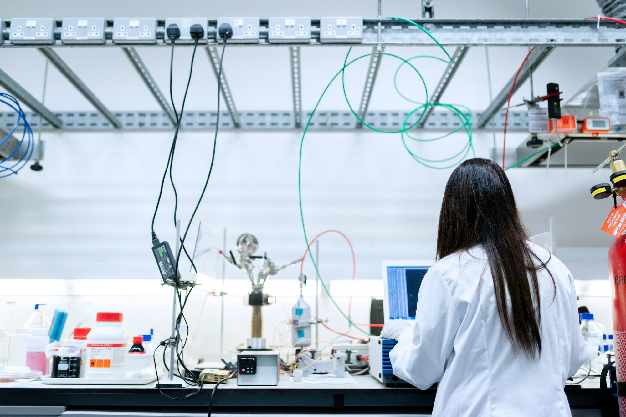
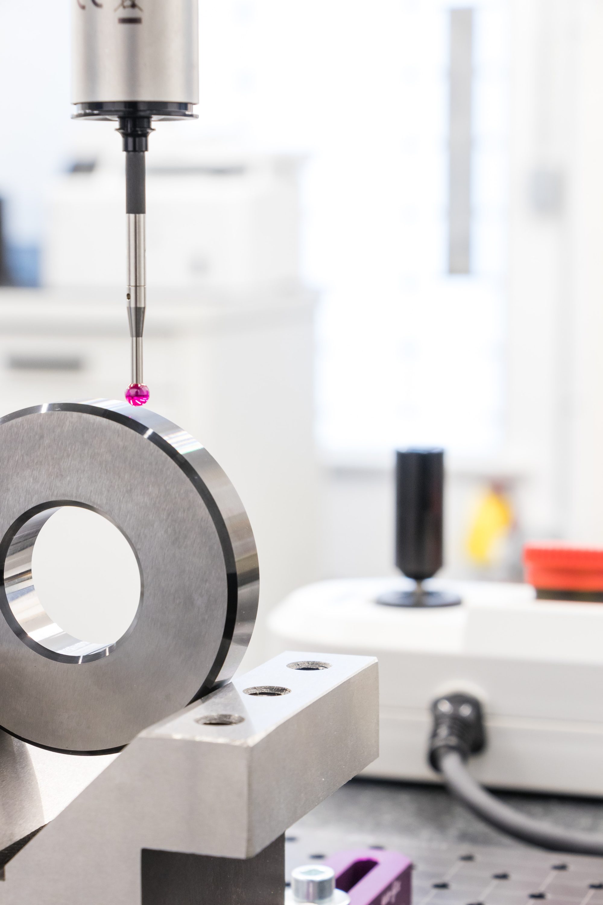
Synthesis and small-scale testing at IMD-1
At the Institute of Energy Materials and Devices (IMD-1) we run our own labs for
projection micro-stereolithography and 3D printing of preceramic polymers,
electrodeposition of nanometallic multilayers, and sample preparation, complemented by
the institute's SEM/EBSD, X-ray diffraction, thermochemistry, and nanoindentation
facilities.
This combination lets us take a material all the way from synthesis through
microstructure to mechanical and functional properties - and back, closing the loop
between processing and atomic-scale characterization.
Electron microscopy at the Ernst Ruska-Centre
Through the ER-C we work on aberration-corrected instruments including a probe-corrected
Titan ChemiSTEM (HAADF-STEM, EDX, 4D-STEM), a monochromated Titan Spectra for
high-resolution EELS down to the Li-K edge, a Tescan Tensor for precession-assisted
4D-STEM, and a Talos F200X G2 for analytical STEM and tomography.
In-situ heating, biasing, and deformation experiments run on MEMS-based holders, and
site-specific specimens are prepared on a Helios 5 plasma FIB with EBSD, TKD, and
ToF-SIMS.
Forschungszentrum Jülich
Forschungszentrum Jülich (abbreviated to FZJ) is a national research institution for interdisciplinary research in the fields of energy, information and bioeconomy. With around 7,200 employees (2023) in eleven institutes and 80 institute divisions, it is one of the largest research facilities in Europe.
fz-juelich.de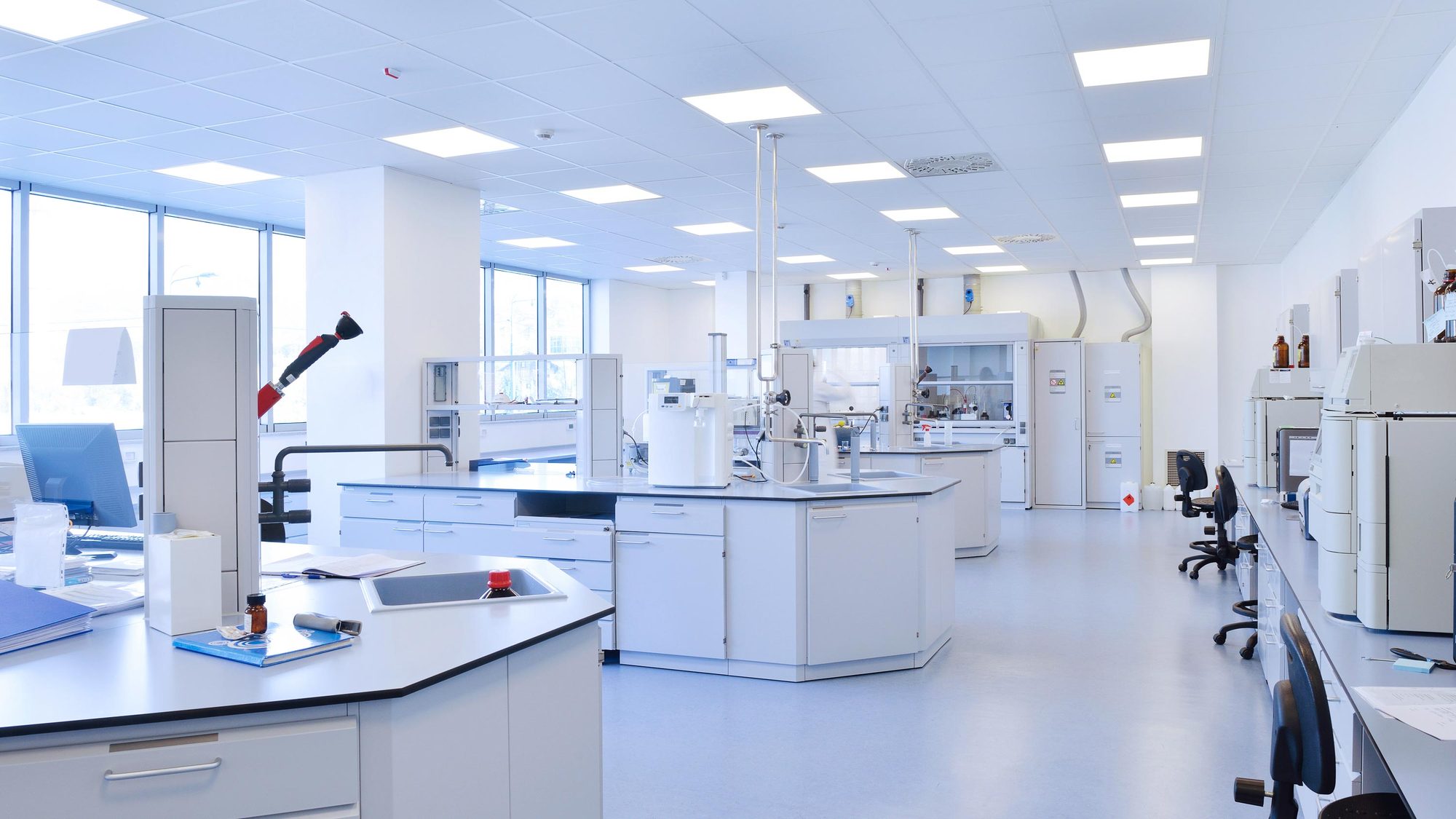
Our Partners
Long-standing collaborations connect the group to materials science institutes across Europe and the US.


Austrian co-PI of the DFG-FWF Weave project SISTer; high-temperature micromechanics of ultrafine-grained tungsten alloys.
Grain boundary structure and segregation, atom probe tomography, and hydrogen micromechanics.


PVD thin-film deposition and atom probe tomography of combinatorial Ni-Al films.


Co-sputtered combinatorial thin films and nanoscale metallic multilayers.


PVD and ALD multilayer deposition for interface-dominated model systems.